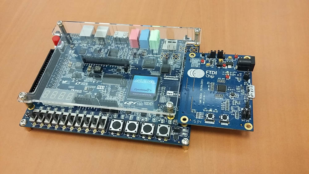
Terasic Cyclone 5 GX Starter Kit
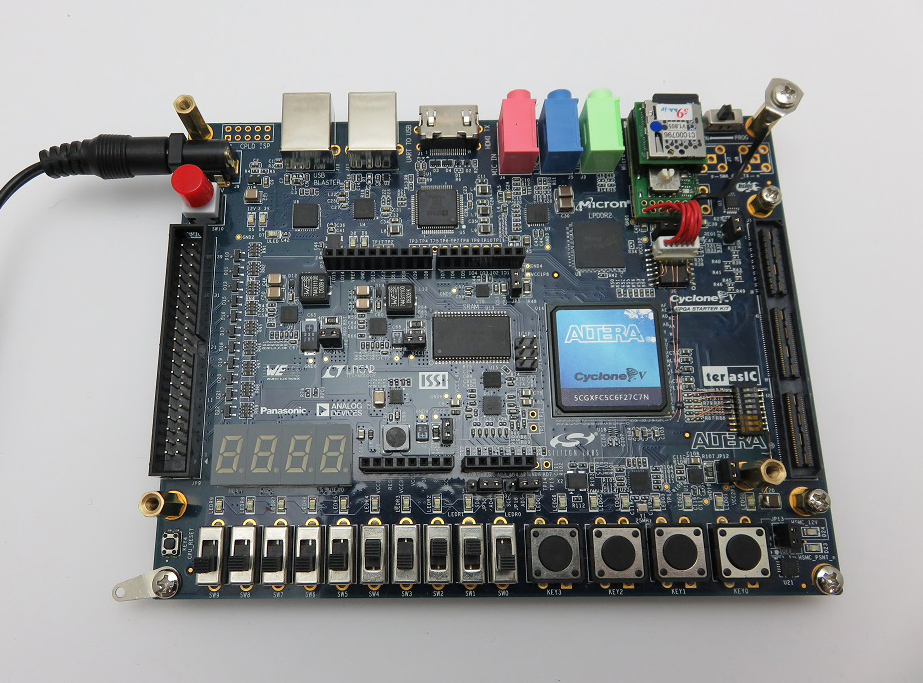
Terasic Cyclone 5 GX Starter Kit development board
The C5GX is an FPGA board based on the Altera Cyclone 5 without SoC
Main Features :
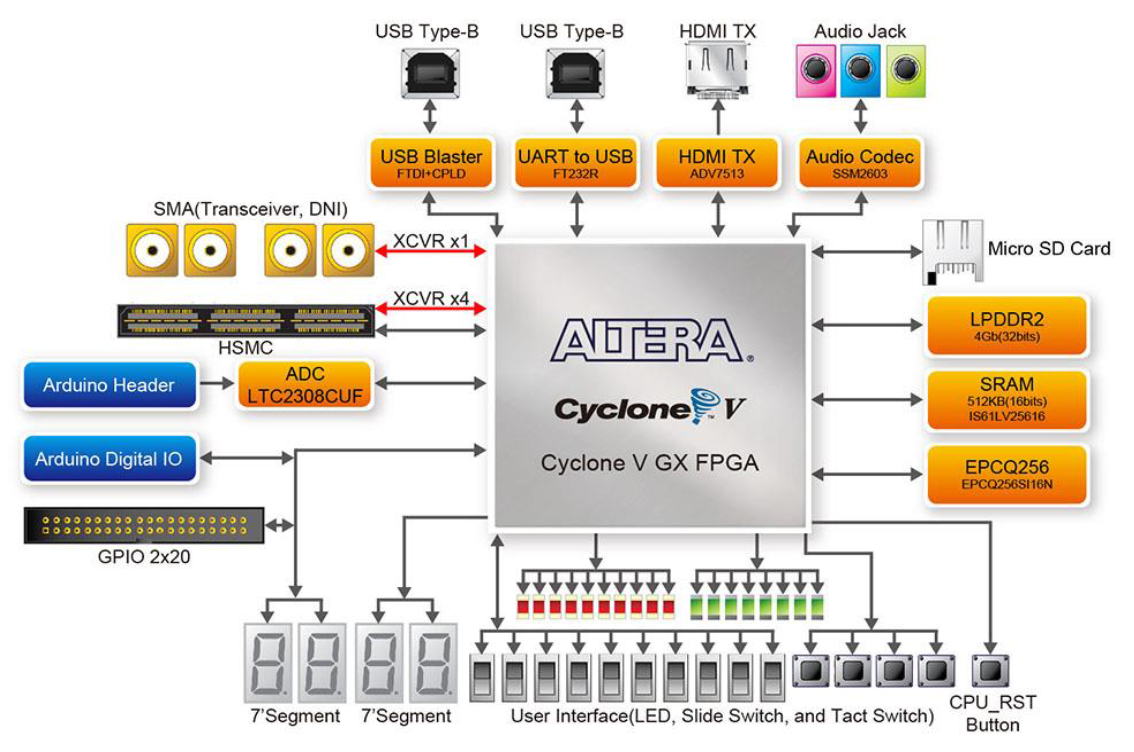
- FPGA Device
Cyclone V GX 5CGXFC5C6F27C7N Device
77K Programmable Logic Elements
4884 Kbits embedded memory
Six Fractional PLLs
Two Hard Memory Controllers
Six 3.125G Transceivers - Configuration and Debug
Quad Serial Configuration device – EPCQ256 on FPGA
On-Board USB Blaster (Normal Type-B USB connector)
JTAG and AS mode configuration supported - Memory Device
4Gb LPDDR2 x32 bits data bus
4Mb SRAM x16 bits data bus - Communication
UART to USB
Expansion I/O
HSMC x 1, including 4-lanes 3.125G transceiver
2×20 GPIO Header
Arduino header, including analog pins
SMA x 4 (DNI), one-lane 3.125G transceiver - Display
HDMI TX, compatible with DVI v1.0 and HDCP v1.4
- Audio
24-bit CODEC, Line-in, line-out, and microphone-in jacks
Switches, Buttons, LED, and 7-Segments - Others
18 LEDs
10 Slide Switches
4 Debounced Push Buttons
1 CPU reset Push Buttons
Four 7-Segments - Micro SD Card Socket
Provides SPI and 4-bit SD mode for SD Card access
- Power
12V DC input
First impressions :
No CD => can be downloaded from terasIC upon a free registration : informations on data-sheets of the components used, as well as a full schematic of the dev board.
Slower than the DE0Nano as for the speed spec (not a 6 series but a 7 series) Then again it’s for a Cyclone 5 not a Cyclone 4 so it might be still faster, not sure.
No step by step examples, unlike the DE0-Nano.
Pretty beefy power supply 12V 2Amps so not for low power applications. Also I didn’t take the power supply apart (since it’s pretty much glued) so I’m not sure about how safe it is.
Be careful about shared GPIO pins between the GPIO the Arduino header and two of the 7 segment displays.
About the 7 segment displays, there is no wiring for the 8th segment (the dot) but it also seems they left the dots totally unconnected (not even a through hole connector for them as they did for other components).
Unpopulated SMA transceivers (to cut cost probably) but you can get a daughter board (for as much if no more of the cost of the dev kit) for some serious AD/DA converters via the HSMC connector.
Component review :
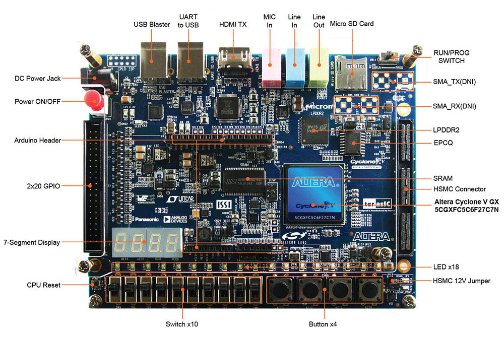
- HDMI
They use an Analog Devices HDMI Transmitter ADV7513 controlled via a serial I2C bus.
HDMI is awesome but they don’t offer direct HDL code samples, it does required a Qsys package with IP modules that require licensing, There are some dependencies on the NIOS soft-core but the actual Verilog that implements that dependency is encrypted so you can’t detach it from the license. That method handles the HDMI_TX_INT that triggers the initialization, hot plug/unplug and other situations, so it’s pretty critical for a full stand alone application.
It could be that they don’t have a good handle on how to implement the HDMI_INT in Verilog or VHDL, so they pass the interrupt to the NIOS soft core to handle it. But you can do your own interrupt handler by following the Analog Devices documents included on the CD under the data-sheets, (downloadable as explained before). Or they don’t want to give away the NIOS interface, or decided people will purchase the license instead of reading the data-sheet to support the hardware, not sure but I tend to go to the later, even if their IP code only deals with the video and not with the audio or 3D configurations.
No audio HDMI. Even if the HDMI transmitter supports it (it also supports 3D and HDCP among other things) The reason for no audio support is that the HDMI transmitter audio pins are not physically connected to the FPGA.
But if you want to use that capability, terasIC actually did us a solid and provided through hole test points that are labelled as test pins on the top of the board, but they have the actual signal names on the bottom silk.
Note the bottom image next to the Arduino power header. On the top image you can see those as TP3-TP11, TP3 being ground and 4-11 the HDMI audio signals/clocks.
The through holes are all lined up with standard spacing, so you can solder a header and connect them to some GPIO pins and then you can write your own HDL to drive it (no IP from them for the sound as far as I can tell). The programming for the HDMI audio supports: I2S, SPDIF or HBR.
You might be able to put a header that doesn’t need to be solder, not sure if the holes will accept prototyping headers and not sure if such beast exists. Something like this for the launchpad that is breakable so you can get rid off the two extra pins and use those for the extra Arduino header analog inputs. (Funny, the bottom picture has the extra two analogs populated, the top view has them not populated)
0.100″ (2.54 mm) Straight Female Header: 1×10-Pin - GPIO
It has a 40pin connector with 36 GPIO pins plus 2 grounds, a 3.3V pin and a 5.0V pin. GPIO_0 & GPIO_2 can also be used as dedicated clock inputs. GPIO_16 & GPIO_18 can also be used as PLL Clock outputs (shared with Arduino header IO_13 & IO_15).
GPIO_3 through GPIO_18 are shared with the Arduino header IO_0 through IO_15.
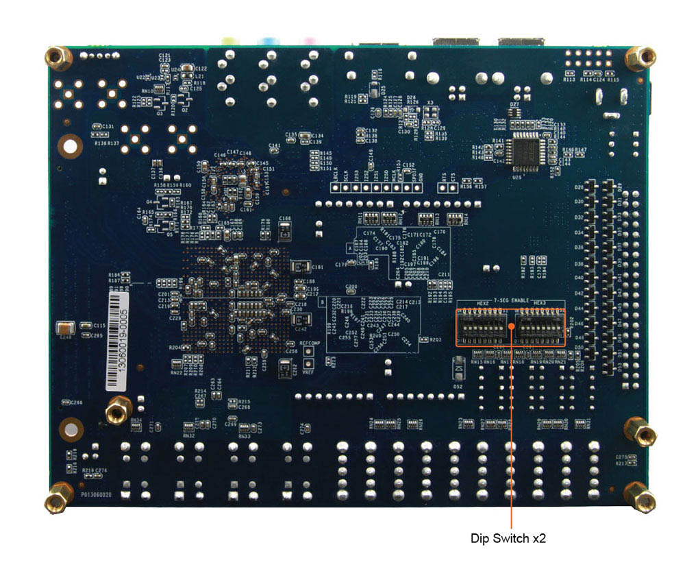
HEX2 and HEX3 (the 7 segment displays) share pins with GPIO_22 through GPIO_35 but it has dip switches in the bottom of the board to disconnect the wires from the two 7 segment displays (one segment at a time).
Funny that the dip switches are count 8 each so one switch per block is not connected (maybe they intended to have the dot after all at one point).
Not sure about this approach, I know it gives you more flexibility but you gotta be very careful if you plan on attaching an Arduino shield. You better make sure the dip switches are off and also you gotta make sure you clear the board configuration so that the sample configuration or your last pof file doesn’t put signals that were intended for the 7 segment display. They do have an executable to delete you configuration file so it won’t drive anything upon boot while transitioning from talking to the Hex upper two digits, or the Arduino data header, or the GPIO. But I can see this being a problem if you don’t pay attention.
Arduino Header
There are two jumpers to change the configuration of the header, it comes with a 12V power pin (I don’t think the Galilleo has it and not sure on the standard Arduino. it comes with an extra 2 analog inputs but there is no header for those two. So it has 6 with the header and I believe the Arduino Uno R3 has 8, but you will have to add the two pin header yourself.
They use an LTC2308 ADC 500ksps, 8-channel, 12-bit. - LEDs
Well, you get 10 red and 8 green. - Buttons
De-bounced and 4 count, nothing to write home about other than they are regular size, not those tiny ones the DE0 Nano has. - Switches
Not to confuse these with the dip switches. The board has 10 slide switches (nice and big, not those tiny ones the DE0 Nano has) - On/Off Button.
Brilliant, no more plugging and unplugging your board. I know they have this before but not on boards at this price, and it’s a nice big red button! - Audio Codec
It comes with Mic-In, Line-In and Line-Out. Didn’t play with this yet but they use an Analog Devices SSM2603 24-bit audio controlled via I2C. Sample rates variable from 8 kHz to 96 kHz. - HSMC
High Speed Mezzanine Card, the connector is very expensive but terasIC has a bunch of HSMC daughter boards that you can put in there, including some impressive DAC/ADC boards with two 14 bit ADC channels up to 150MSPS and two 14 bit DAC that can hit up to 250MSPS and extra audio interface line-in, line-out, headphone & mic. (thinking signal generator don’t know) but at almost $400 I might stick with something cheaper for now.
$200 gives you two 14-bit ADC at 65 MSPS and two 14-bit DAC at 125 MSPS.
But they have other things available like LCD displays, HDMI receivers, Also for $140 you can get a 4 high speed transceiver board.
For example if you want more GPIOs then grab the GPIO-HSTC card for $55 to get 3x 40x connectors (36 GPIO + power/ground)
The socket has 4 transceivers channels on top of the two unpopulated ones on-board.
It also has tons of LVDS RX/TX, 4 differential clocks input and outputs. An I2C bus.
For high speed stuff this would be very useful maybe even drive LCDs directly.
They have also a jumper to enable 12V to be available on the HSMC connector. - LPDDR2 memory
They use some Micron MT42L128M32D1LF-25 WT:A mobile memory chip 4Gb but, have not played with it and how to address it, you have to deal with banks and the configuration is 16 Meg x 32bits x 8 banks.
I think it’s the same memory as what’s on the Raspberry Pi. - SRAM
4Mb (512KB) worth of it, they use an ISSI IS61WV25616 chip with 8 to 10 ns access time. Haven’t done much with that yet. Data width is 16 bits, 18 bit address space. - RS-232 Serial Port to USB interface
Have not used it yet but if your computer doesn’t have RS-232 and you want to control the board after being programmed by this with speeds up to 3Mbps. They use an FT232R chip to do the job. Data-sheet of course comes with the downloadable CD. - Micro SD Card
Supports x4 data lines micro SD cards, also I have not played with this part yet. - EPCQ
(Quad Serial Configuration) devices, it comes with the EPCQ256, this is good to know because if you want to create pof files you must specify this in Quartus II. otherwise you can’t program your board directly with your code. I’m not sure if the template generated by the system builder utility does that for you as well, it might do it.
Program in AS mode so it sticks as opposed of JTAG for programming until you power cycle the board. Meaning without the EPCQ256 setting under assigments/device…/Device and Pin Options…/Configuration/Configuration Scheme set to Active Serial x4 and set the Configuration device to EPCQ256, it won’t generate the pof file needed to flash your board. - RUN/PROG Switch
This allows you to download the code in AS mode via the EPCQ instead of temporarily via the JTAG interface. - USB Blaster
To program your board it has it built in so you don’t need to purchase the programmer separately. - CPU Reset
Oh, yeah, I almost forgot, it as a tiny micro switch labelled CPU reset that you can use it as a reset if you configure your board to use it. - Misc
The I/O pins can be configured like other Altera FPGAS Giving you a lot of flexibility.
Not sure if it’s 5V I2C tolerant but if it’s not, there are ways to solve that. I did post a link to a Philips service note a while back that adafruit is maintaining.
Edit link: Bi-directional level shifter for I²C-bus and other systems.
Conclusion :
Only 77K logic elements is enough to experiment and learn.
Leave a reply