Tag Archives: fpga

FTDI Morph-IC-II

FTDI Morph IC II

FTDI Morph IC II block diagram

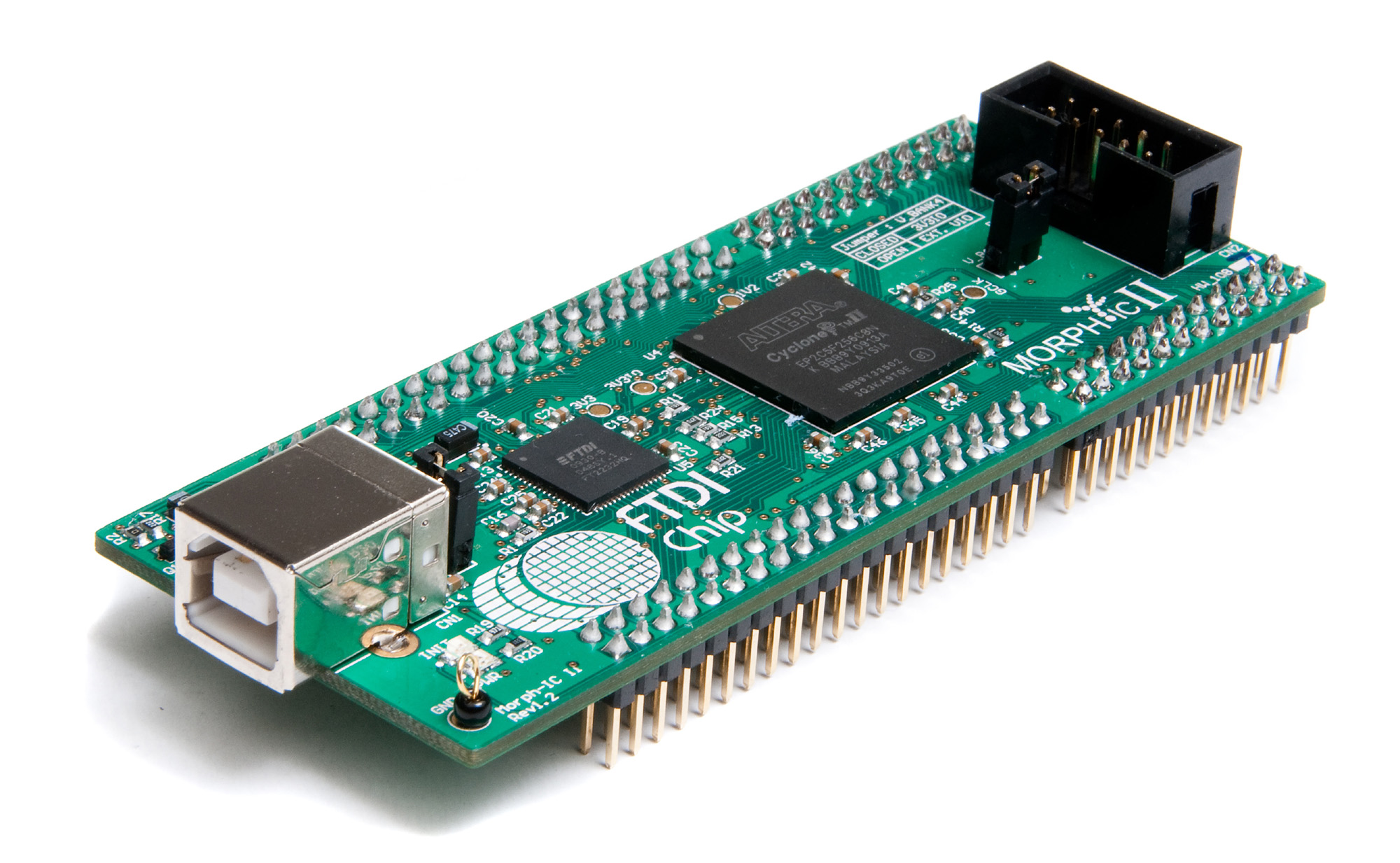
FTDI Morph-IC-II FPGA development board

The Morph-IC-II is an FPGA board based on the Altera Cyclone 2

Main Features :

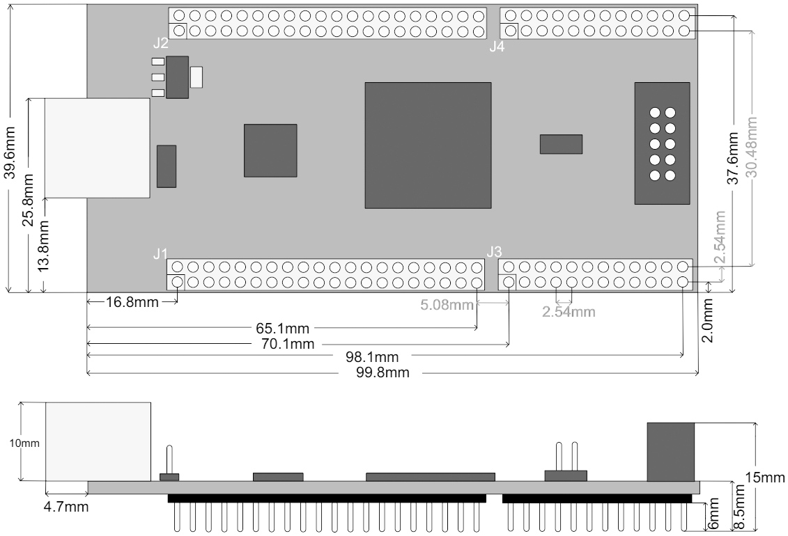
  • 105mm x 40mm board size
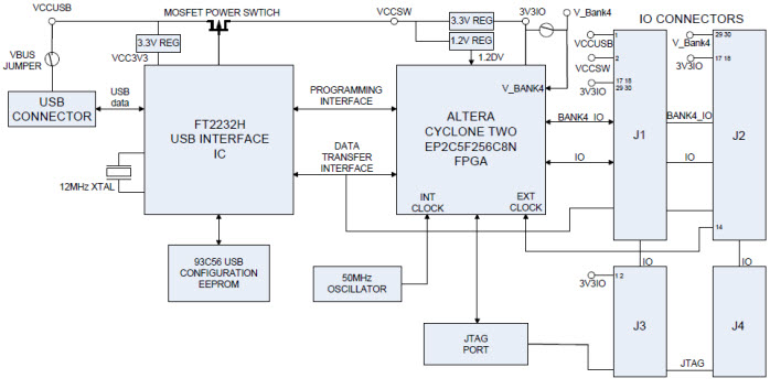
  • FT2232HQ Dual, Hi-Speed USB UART/FIFO IC used for USB communications
  • Altera Cyclone 2 – EP2C5F256C8N FPGA capable of synthesizing large scale integrated circuits
  • Ultra fast FPGA configuration/reconfiguration over USB (under 0.1 sec)
  • 4,608 Embedded FPGA Logic Elements (about 80,000 Gates typically)
  • 26 Embedded Logic RAM Elements (119Kbits)
  • FPGA-PC USB Data Transfer at up to 40MByte/sec
  • Onboard 93LC56B configuration EEPROM
  • MOSFET switched 5V and 3.3V power outputs for powering external logic
  • Onboard 12MHz crystal and essential support components for FT2232HQ
  • 80 dedicated external I/O pins
  • Onboard 50MHz oscillator as FPGA primary clock – also available for external use
  • JTAG interface for testing the I/Os and registers of the FPGA
  • 1 dedicated external clock input
  • Powered from USB bus or external PSU
  • Standard 0.1 inch pitch format connector pins, ideal for rapid prototyping or small-medium size production runs
  • FTDI’s VCP and D2XX USB Windows and Linux USB drivers (provided) eliminate the need for driver development in most cases
  • FPGA loader interface DLL (for Windows only not including CE) supplied including interface examples in VB, VC++ and Delphi
  • Stand-alone FPGA loader programs provided for Windows and Linux
  • VHDL programming examples (I/O over USB) provided
  • Delphi application software examples including source code provided
  • Free Altera Quartus II Software Starter Suite development software available from the Altera Website
  • Backward compatible with the existing MorphIC-I
  • Supports 1.5/1.8/2.5/3.3-V LVTTL/LVCMOS signals, IOBANK1-3 restricted to 3.3V
FTDI Morph-IC-II dimensions :
FTDI Morph IC II dimensions
Morph-IC-II is a compact and powerful FPGA module which is capable of implementing LSI (Large Scale Integration) designs or entry level VLSI (Very Large Scale Integration) designs.

Designs can be synthesised through utilising up to 4,608 Logic Elements of Morph-IC-II‟s on board FPGA.

The Morph-IC-II platform combines an Altera Cyclone®-II FPGA with high-performance USB 2.0 capabilities that facilitate Hi-speed communications with ultra-fast, sub-100ms FPGA programming/reprogramming.

This makes Morph-IC-II ideal for applications which require users to reconfigure hardware functionality “on-the-fly” by downloading new software over USB : “morphing” the hardware.

Communication between the FPGA and the PC is done through a USB 2.0 connection to the FTDI FT2232H USB 2.0 Hi-Speed (480Mbit/s) USB bridge. Morph-IC-II is an easy to use module which allows users to program and interact with the FPGA using a free software package produced by Altera called Quartus II.

RedPitaya V1.1 Board

RedPitaya Top

RedPitaya Bottom

RedPitaya Block Diagram

RedPitaya Board V1.1 Board

Red Pitaya is an open-source-software measurement and control tool that consists of easy-to-use visual programming software and free of charge, ready-to-use open-source, web-based test and measurement instruments.
With a single click, the board can transform into a web-based oscilloscope, spectrum analyzer, signal generator, LCR meter, Bode analyzer, or one of many other applications.
Red Pitaya can be controlled by using Matlab, LabView, Python & Scilab.

RedPitaya Ressources

Main Features :

  • Dimensions: 107 mm x 60 mm x 21 mm
  • Ethernet 1Gbit/s (PHY Intel-Lantiq PEF7071V V1.5 10/100/1000Mbps)
  • USB 2.0 (Microchip-SMSC USB3320C)
    • OTG (On-The-Go, can work without host)
    • WiFi USB dongles is possible : tested with Edimax EW­7811Un
  • 2x SMA RF inputs
    • Bandwidth : 50 MHz (3 dB)
    • Input impedance : 1 MΩ // 10 pF
    • Sample rate : 125 Msps
    • ADC resolution 14 bits
    • Full scale voltage : +/-1V or +/-20V
    • Absolute maximum input voltage rating : 30V (1500V ESD)
  • 2x SMA RF outputs
    • Bandwidth : 50 MHz (3 dB)
    • Sample rate : 125 Msps
    • DAC resolution : 14 bits
    • Load impedance : 50 Ω
    • Output slew rate limit : 200 V/us
  • Serial connectivity (Daisy Chain)
    • Connector type : 2x SATA type connector
    • Two differential pairs per connector enabling up to 500 Mbps
  • FPGA: Xilinx Zynq 7010 SoC
    • 17,600 LUTs
    • 28k Logic Cells
    • 80 DSP slices
    • Dual ARM® Cortex™­A9
  • Memory: 4 Gb DDR3 SDRAM (512 MB)
  • SD card
    • Card type: micro SD
    • Supported standard: SD/SDIO 2.0/MMC3.31
    • File System: FAT32
    • Maximum card size: 32 GB
  • 5V 2A micro USB Power supply
RedPitaya Extension Connectors
2x Extensions Connectors 26 pins HE10 (E1 & E2) :

  • 4x Auxiliary analog input channels
    • Connector : dedicated pins on IDC connector E2 (pins 13,14,15,16)
    • Nominal sampling rate : 100 ksps
    • ADC resolution 12 bits
    • Input voltage range : 0 to +3.5 V
  • 4x Auxiliary analog output channels
    • Output type : Low pass filtered PWM
    • PWM time resolution : 4ns (1/250 MHz)
    • Output voltage range : 0 to +1.8V
  • 16x GPIO
    • Voltage level : 3.3V
    • Direction : configurable
    • 16 single ended or 8 differential digital I/Os with 3,3V logic levels
  • I²C, UART, SPI
RedPitaya Case
RedPitaya Plastic Case

RedPitaya Kit
RedPitaya Kit

RedPitaya Oscilloscope
RedPitaya Oscilloscope on iPad

RedPitaya System
RedPitaya System

RedPitaya Visual Programming

RedPitaya’s Visual Programming is equivalent of Lego, and is similar to “MIT Scratch” programming, that means that RedPitaya is more for fun than for professional applications.
RedPitaya Extension Module Top

RedPitaya Extension Module Bottom

RedPitaya Extension Modules

RedPitaya’s extension module board (~25 euros) is able to measure for example temperature, vibration or movement with special mini-modules connected on it. This mezzanine board facilitates the quick connection of different sensors and actuators to the Red Pitaya. All the “Grove modules” of “Seeed Studio” are available to connect it.

Linera FMU3-S651 Board

Linera FMU3 S651 Top

Linera FMU3-S651 – USB3 development board

The Linera FMU3-S651 is a USB 3.0 integration module based on the Spartan 6, able to get a performance over 340 MiB/s

Main Features :

  • 65mm x 50mm board size
  • USB 3.0 Connectivity, including software drivers and APIs
  • Cypress EZ-USB FX3 – 100 MHz 32b data bus to a USB 3.0 port
  • Xilinx Spartan6 LX45 application FPGA (Available also with LX150)
  • 1Gbit DDR3 SDRAM (Optional 2 or 4 Gbit)
  • MicroSD card slot, accessible from FPGA
  • Very easy to integrate: Single 5V supply
  • Programmable via USB 3.0 port, JTAG or the on-board flash
  • Two Samtec RAZOR BEAM™ LSHM pitch 0.5mm high speed board-to-board connectors to mount on a host-board
  • 148 user I/O signals. 71 differential pairs
  • 8 User LEDs on-board
  • Pin-compatible with FM-S651 series
  • On-board, programmable clock generator with 3 output clocks, with available SSC
  • Breakout board available
Linera FMU3 S651 Block diagram
USB3 CONNECTIVITY
FMU3 series FPGA modules are equipped with a USB3.0 port.
The on-board FPGA can communicate with a host PC through the USB 3.0 port with unprecedented speed (~340MB/sec sustained transfers)

EASY INTEGRATION
FMU3 series FPGA modules can be mounted on a carrier board using 2 high-speed connectors.
There are 148 IO pins available to the end-user.
The board is supplied with drivers and API for easy USB 3.0 communication with a PC.

FLEXIBILITY
The on-board FPGA on FMU3 series modules can be programmed via the USB port, via JTAG or via the on-board Flash. There is a Micro-SD card slot accessible via the FPGA and 1Gbit DDR3 SDRAM.

Linera FMU3-S651 Daughter Board example :
Linera FMU3 S651 Daughter Board1
Linera FMU3-S651 Daughter PCB example :
Linera FMU3 S651 Daughter Board2

Cesys EFM02 USB3 Board

Cesys efm02 top

EFM02 – USB3 development board

Spartan-6 FPGA module, DDR2 SDRAM, Flash and superspeed USB 3.0 interface

Main Features :

  • SUPERSPEED USB 3.0
  • 2Gbit DDR2
  • Up to 191 user IO
  • Xilinx Spartan-6LX® FPGA
    versions available:
    XC6SLX45-3FGG484I
    XC6SLX100-3FGG484I
    XC6SLX150-3FGG484I
  • 64Mbit dual SPI flash
  • USB3 controller : CYPRESS™ FX3
  • EFM02-45-3I (XC6SLX45-3FGG484I) Price : 420$
Block diagram is the following :
Cesys efm02 Block diagram
Cesys efm02
Cesys efm02 bot
All Features

  • USB3.0 SuperSpeed interface through versatile CypressTM EZ-FX3 controller
  • USB bus-powered, no external power supply necessary
  • Optional self-powered mode available
  • 32bit Slave FIFO interface
  • Two FX3 GPIO on expansion connector
  • XilinxTM Spartan-6 FPGA (LX45, LX100 or LX150)
  • Up to 191 single-ended (95 differential) IOs on high-quality high-speed SamtecTM
    connectors (QSE-060-01), including several GCLK inputs
  • 157 single-ended (78 differential) IOs identical throughout EFM-02B line-up
  • Independent power supply option for FPGA bank 0 and/or bank 1
  • 2Gbit DDR2 memory
  • 64Mbit dual SPI configuration/data memory
  • High stability 100MHz +/-25ppm onboard clock oscillator
  • Mounting position for optional user clock oscillator (industry standard 5mm*7mm)
  • 1Mbit (512kbit1) I²C EEPROM for FX3 configuration data
  • I²C interface available on expansion connector to increase available FX3 configuration memory for standalone applications
  • FPGA configuration from SPI memory, JTAG or USB
  • One user, two status leds
  • JTAG for FPGA and FX3 controller available on expansion connectors
  • Small sized PCB only measures 52,6mm x 82,6mm
Breakout board :
Cesys efm02 breakout board
Features :

  • HSMC to HE10 connectors
  • PCB has two layers, not for high-speed applications
  • Price : 75$

OpalKelly USB3 Altera Board

OpalKelly ZEM4310

Zem4310 – USB3 development board

The ZEM4310 is a USB 3.0 integration module based on the Altera Cyclone IV FPGA (55kLE), able to get a performance over 340 MiB/s

Main Features :

  • SUPERSPEED USB 3.0
  • 128 MiB DDR2
  • BOOTABLE SERIAL FLASH (2x 16 MiB)
  • SWITCHING POWER SUPPLIES
Block diagram is the following :
OpalKelly ZEM4310 Block diagram
All Features :

  • Altera Cyclone IV FPGA (EP4CE55F23C8N)
  • 2x 32-MiB serial flash (Numonyx N25Q128A)
  • 128-MiByte DDR2 (Micron MT47H64M16HR)
  • Small form-factor, smaller than a credit card at 80mm x 60mm x 15.98mm (3.15″ x 2.36″ x 0.63″)
  • High-speed USB 3.0 interface (Cypress FX3) for configuration and data transfer
  • Measured performance over 340 MiB/s
  • Self-powered by external DC source
  • 50 MHz clock oscillator
  • Two LEDs
  • Two HSMC-compatible 180-pin 0.5mm Samtec board-to-board connectors (QSH-090)
  • Over 160 user I/O and 4 GCLK pins on expansion connectors
  • Full FrontPanel virtual control panel support
  • Complete Application Programmer’s Interface (API) in C, C++, C#, Ruby, Python, and Java
OpalKelly ZEM4310 Bottom
HSMC Bottom connectors :

  • Two HSMC-compatible 180-pin 0.5mm Samtec board-to-board connectors (QSH-090)
  • Over 160 user I/O and 4 GCLK pins on expansion connectors
OpalKelly ZEM4310 Slide